
Power mosfet smd 110v STC2326
dapatkan harga terkini| Jenis bayaran: | L/C,T/T,Paypal |
| Incoterm: | FOB,CFR,CIF |
| Pengangkutan: | Ocean,Air |
| Port: | SHANGHAI |

| Jenis bayaran: | L/C,T/T,Paypal |
| Incoterm: | FOB,CFR,CIF |
| Pengangkutan: | Ocean,Air |
| Port: | SHANGHAI |
Model No.: YZPST-STC2326
Jenama: YZPST
B TA30 Siri Triacs
YZPST-STC2326
DESKRIPSI
STC2326 adalah mod peningkatan kuasa logik N-Channel transistor kesan kuasa medan yang dihasilkan menggunakan teknologi tren parit DMOS ketumpatan super yang tinggi. STC2326 telah direka khusus untuk meningkatkan kecekapan keseluruhan penukar DC / DC yang menggunakan pengawal PWM beralih segerak atau konvensional. Ia telah dioptimumkan untuk caj pintu rendah, RDS rendah (ON) dan kelajuan pensuisan pantas.
APLIKASI
Sistem Powered
DC / DC Converter
Suis Beban
CIRI-CIRI
110V / 3A, RDS (ON) = 310mΩ @ VGS = 10V
Reka bentuk sel ketumpatan tinggi untuk RDS yang sangat rendah (ON)
Keupayaan rintangan luar biasa dan keupayaan maksimum DC semasa
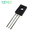
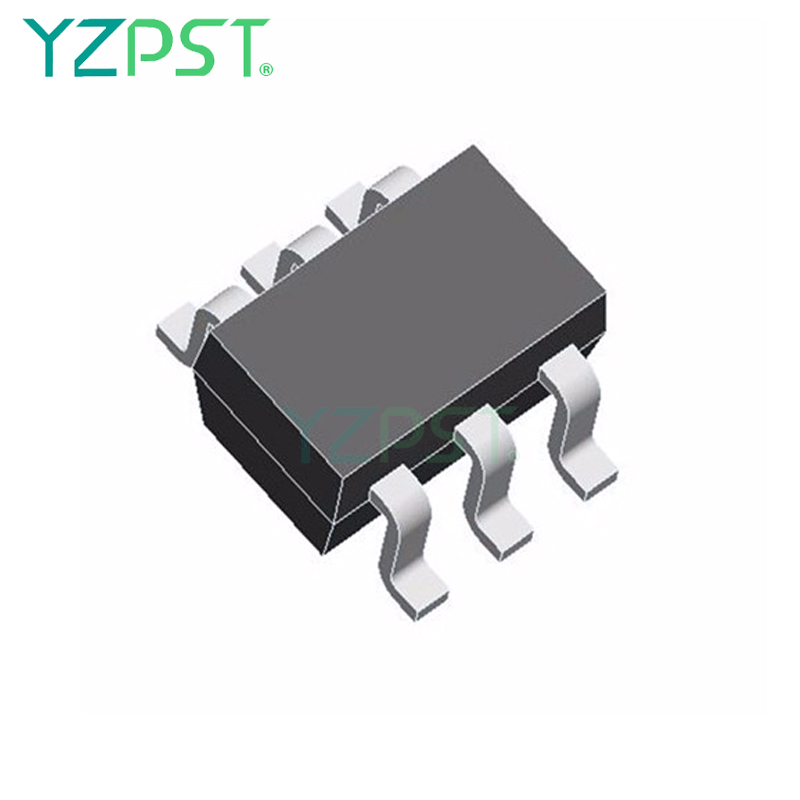
Reka bentuk pakej SOT-23-6L
PIN CONFIGURATION (SOT-23-6L)
")
|
Pin |
Symbol |
Description |
|
1 |
D |
Drain |
|
2 |
D |
Drain |
|
3 |
G |
Gate |
|
4 |
S |
Source |
|
5 |
D |
Drain |
|
6 |
D |
Drain |
O RDER ING DALAM F O R M A T I O N
|
Part Number |
Package |
Part Marking |
|
SPN2326S26RGB |
SOT-23-6L |
26YW |
A B SOU L T E MA X I M U M R A T DI G S ( T A = 25 ℃ U n l e s s o t h e r w i s e n o t d d )
|
Parameter |
Symbol |
Typical |
Unit |
|
|
Drain-Source Voltage |
VDSS |
110 |
V |
|
|
Gate –Source Voltage |
VGSS |
±20 |
V |
|
|
Continuous Drain Current(TJ=150℃) |
TA=25℃ |
ID |
3.0 |
A |
|
TA=70℃ |
2.0 |
|||
|
Pulsed Drain Current |
IDM |
10 |
A |
|
|
Power Dissipation |
TA=25℃ |
PD |
2.0 |
W |
|
TA=70℃ |
1.3 |
|||
|
Operating Junction Temperature |
TJ |
-55/150 |
℃ |
|
|
Storage Temperature Range |
TSTG |
-55/150 |
℃ |
|
|
Thermal Resistance-Junction to Ambient |
RθJA |
62.5 |
℃/W |
|
|
Parameter |
Symbol |
Conditions |
Min. |
Typ |
Max. |
Unit |
|
Static |
||||||
|
Drain-Source Breakdown Voltage |
V(BR)DSS |
VGS=0V,ID=250uA |
110 |
|
|
V |
|
Gate Threshold Voltage |
VGS(th) |
VDS=VGS,ID=250uA |
1 |
2.0 |
2.5 |
|
|
Gate Leakage Current |
IGSS |
VDS=0V,VGS=±20V |
|
|
±100 |
nA |
|
Zero Gate Voltage Drain Current |
IDSS |
VDS=80V,VGS=0V |
|
|
1 |
uA |
|
VDS=80V,VGS=0V TJ=125℃ |
|
|
5 |
|||
|
On-State Drain Current |
ID(on) |
VDS≥5V,VGS =10V |
3.0 |
|
|
A |
|
Drain-Source On-Resistance |
RDS(on) |
VGS= 10V,ID=3A |
|
0.26 |
0.31 |
Ω |
|
Forward Transconductance |
gfs |
VDS=10V,ID=3A |
|
2.4 |
|
S |
|
Diode Forward Voltage |
VSD |
IS=1A,VGS =0V |
|
|
1.2 |
V |
|
Dynamic |
||||||
|
Total Gate Charge |
Qg |
VDS=80V,VGS=10V ID= 5A |
|
9 |
13 |
nC |
|
Gate-Source Charge |
Qgs |
|
2 |
|
||
|
Gate-Drain Charge |
Qgd |
|
1.4 |
|
||
|
Input Capacitance |
Ciss |
VDS=25,VGS=0V f=1MHz |
|
508 |
|
pF |
|
Output Capacitance |
Coss |
|
29 |
|
||
|
Reverse Transfer Capacitance |
Crss |
|
16.5 |
|
||
|
Turn-On Time |
td(on) |
VDD=50V,RL=10Ω ID=3A,VGEN=10V RG=3.3Ω |
|
2 |
|
nS |
|
tr |
|
21.5 |
|
|||
|
Turn-Off Time |
td(off) |
|
11.2 |
|
||
|
tf |
|
18.8 |
|
|||
")
")


Tel: 86-514-87782298
Whatsapp: +8613805278321
Alamat: 3rd Floor, Weiheng Building No.20 B Area, Yangzhou, Jiangsu China
Laman web: https://ms.yzpst.com


Privacy statement: Your privacy is very important to Us. Our company promises not to disclose your personal information to any external company with out your explicit permission.
Fill in more information so that we can get in touch with you faster
Privacy statement: Your privacy is very important to Us. Our company promises not to disclose your personal information to any external company with out your explicit permission.